国内哪个院校可以对外做STEM EDS的maping?
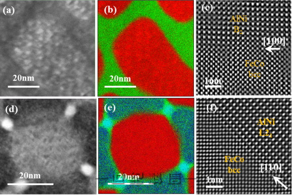
(a) HAADF STEM image, (b) corresponding EDX elemental mapping (red, Fe–Co; green, Al–Ni–Co) and (c) high-resolution HAADF image of alnico 5–7 (transverse) taken close to the [100] zone axis. (d) HAADF STEM image, (e) corresponding EDX elemental mapping (red, Fe–Co; green, Al–Ni; dark blue, Al–Ti–Co; light blue, Cu) and (f) high-resolution HAADF image of alnico 9 (transverse) taken close to the [100] zone axis. (For interpretation of the references to colour in this figure legend, the reader is referred to the web version of this article.)
Q:
请问国内哪里的院校可以对外做STEM(扫描透射电子显微镜)的EDS(能谱)的maping?
A:
为什么一定要STEM?TEM的不行么?
按理来讲,有些TEM上也有STEM模块的
鉴于EDS mapping比较慢,有条件的话还可以做EF-TEM mapping,快而且分辨率也不错
沈阳金属所肯定有设备
洛阳725所第六研究室
引用: 沈阳金属所肯定有设备
金属所确实有,但是做不出来想要的结果,设备出了问题!
回复: 洛阳725所第六研究室
打电话问了,他们只能用扫描电镜做,这个恐怕暂时满足不了我们的需求
产品目录
- 三维面检测系统
- 应力测量系统
- 晶圆翘曲测量系统
- 正置荧光显微镜
- 明暗场显微镜
- 落射照明显微镜
- 暗场显微镜
- 荧光激发光源
- 金相耗材
- 光学原子力显微镜一体机
- 磨平机
- 物证检验仪
- 切割机
- 低速切割机
- 刑侦显微镜
- 三目金相显微镜
- 工业显微镜
- 视频显微镜
- 科研级数码生物显微镜
- 双目偏光显微镜
- 三目偏光显微镜
- 偏光显微镜
- 单目生物显微镜
- 导星相机
- 显微镜电子目镜
- 制冷CCD摄像头
- 显微镜制冷CCD
- 制冷CCD
- 生物显微镜
- Labomed显微镜接口
- 万向支架体视显微镜
- C接口相机
- 薄膜微孔显微镜
- 金属表面观察显微镜
- 透反射金相显微镜
- 金相组织分析仪
- 金相组织分析仪器
- 材料分析显微镜
- 现场金相显微镜
- 金相组织检查显微镜
- 数码金相显微镜
- 三目正置金相显微镜
- 金相显微镜
- 手机维修显微镜
- 种子检查筛选显微镜
- 刑侦检测显微镜
- 数码体视显微镜
- 三目体视显微镜
- 定档变倍体视显微镜
- 双目体视显微镜